PCB etching notes in English
aus Metalab Wiki, dem offenen Zentrum für meta-disziplinäre Magier und technisch-kreative Enthusiasten.
Version vom 1. Mai 2011, 21:00 Uhr von Chrysn (Diskussion | Beiträge) (an image donation from the hsc2011 project)
(As an English-speaking, non-German-speaking visitor to Metalab I thought I'd add a few notes from my experience making a PCB using Metalab facilities. -- follower)
- You can use Google Translate to get an idea of what the German language PCB creation instructions say.
- You can probably find a number of English language UV etching guides online that you can use alongside the translated Metalab specific instructions. I used one from ladyada which was somewhat appropriate.
- I used Kicad to produce the Gerbers and then used [1] to create a 600 DPI PNG file. I'm not sure if more recent versions of Kicad produce usable print files or not.
- I would be inclined to increase the width of both signal and power traces. Also, for SMD ICs I would increase the length of the non-connected pads to make soldering them by hand easier.
- I used GIMP to lay-up multiple copies of the board to be etched in one file. On the CAD station it's in German language but the pretty icons help.
- I printed on transparency twice. I followed ladyada's advice and printed it mirrored to minimise the possibility for light to enter from the side when exposing.
- The copper board I found was roughly 100mm x 160mm.
- There are white lab coats hanging on the back of the door to the "chemistry lab"--you will look particularly menacing when they are accessorised with black gloves.
- The UV light has two rocker switches on the left hand side. One controls On/Off and the other controls IR/IR+UV. You want the IR+UV option. And on.
- After exposure you should be able to faintly see the track outline in a light yellow colour on the board.
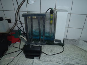
- The etching tank took more than ten minutes to heat.
- Once in the etching tank you should see a colour change (the non-resist area will turn an orangey colour) within a couple of minutes--these are not the colour change you are looking for. Take my word for it. You can confirm this by testing the complete conductivity of the board with a multimeter.
- After multiple stops and starts it took maybe 15-20 minutes to etch the board. Once the copper finally starts to disappear (and you see the fibre glass colour) it is quite rapid however. Keep an eye on it and maybe re-orientate the board to ensure even coverage.
- Don't use the mill bits from the drawers under the CNC/RepRap machine. Try looking in the very thin drawer at the top left of the tool drawers for drill bits. Try 0.8mm size. Drill carefully. Be prepared to buy more. :-)
My project log which includes photographs of my etching: [2]
Have fun!
